

Multilayer PCB Manufacture High Quality Professional Oem Pcb


Related Products
-
 Multilayer Fr4 94vo Pcb Oem FactoryNegotiableMOQ: 1 Piece
 -
Multilayer DIY Fpcb / Printed Circuit Board OemNegotiableMOQ: 1 Piece
-
Circuit OEM/ODM UPS Circuit Pcb Made in ChinaUS$ 1 - 8MOQ: 1 Piece
-
Wifi Circuit Board & Radio Circuit Board Made in ChinaUS$ 1 - 8MOQ: 1 Piece
-
High Quality Motor Control Pcb/Toy Remote Control Car Pcb/Micro SD PcbUS$ 1 - 8MOQ: 1 Piece
Specifications
1.Pcb Manufacture2.UL,SGS,ROHS Certificated
3.OEM&ODM are welcome
4.X-ray&AOI Test
5.Fast Delivery
Welcome To Moko.
----Moko_over 10 years professional PCB & PCB Assembly Manufacturer in China.
Quality First!
Customers First!
Making you more successful!
1. PCB fabrication.
2. One-stop PCBA: PCB+components sourcing+SMD and through-hole assembly
3. PCB clone, PCB reverse engineering.
Our advantage:
1. Free programming and free functional test, free package.
2. High quality: E-test, X-ray, AIO test, QC, 100% funtional test.
3. Professional service. ISO SMT and through hole assembly, over 10 years experience.
4. Warranty period: 2 years.
MOKO TECHNOLOGY LTD
was founded in 2001, located in Shenzhen. We mainly offer Electronics Assembly Service. From our ISO9001:2008 certified factory, we turn out up to 10000 square meter of PCBs and 400000 PCBAs monthly. For assembly, utilizing 8 high-speed SMT lines from Yamaha and Sony, to meet customers' need.
Moko atended exhibitions,EXPO 2012 Munich, EXPO 2014 Moscow,EXPO 2014 Munich, HK Electronic Fairs,et
PCB Technical Specification
| Order Quantity | 1-500,000 |
| Layer | 1,2,4,6,upto 18 layer |
| Material | FR-4,glass epoxy,FR4 High Tg,Rohs compliant,Aluminum,Rogers,etc |
| PCB type | Rigid,flexible,rigid-flexible |
| Shape | Any shape: Rectangular,round,slots,cutouts,complex,irregular |
| Max PCB dimensions | 20inch*20inch or 500mm*500mm |
| Thickness | 0.2~4.0mm, Flex 0.01~0.25'' |
| Thickness tolerance | ± 10% |
| Copper thickness | 0.5-4 oz |
| Copper thickness tolerance | ± 0.25oz |
| Surface finish | HASL,Nickle,Imm Gold,Imm Tin,Imm Silver,OSP etc |
| Solder mask | Green, red,white,yellow,blue,black, Double-sided |
| Silk screen | White,yellow,black,or negative, Double-sided or single-sided |
| Silk screen min line width | 0.006'' or 0.15mm |
| Min drill hole diameter | 0.01'',0.25mm.or 10 mil |
| Min trace/gap | 0.075mm or 3mil |
| PCB cutting | Shear,V-score,tab-routed |
PCB Assembly Capabilities
| One-stop PCBA | PCB+components sourcing+assembly+package |
| Assembly details | SMT and Thru-hole, ISO lines |
| Lead Time | Prototype: 15 work days. Mass order: 20~25 work days |
| Testing on products | Flying Probe Test, X-ray Inspection, AOI Test, functional test |
| Quantity | Min quantity: 1pcs. Prototype, small order, mass order, all OK |
| Files we need | PCB: Gerber files(CAM, PCB, PCBDOC) |
| Components: Bill of Materials(BOM list) | |
| Assembly: Pick-N-Place file | |
| PCB panel Size | Min size: 0.25*0.25 inches(6*6mm) |
| Max size: 20*20 inches(500*500mm) | |
| PCB Solder Type | Water Soluble Solder Paste, RoHS lead free |
| Components details | Passive Down to 0201 size |
| BGA and VFBGA | |
| Leadless Chip Carriers/CSP | |
| Double-sided SMT Assembly | |
| Fine Pitch to 0.8mils | |
| BGA Repair and Reball | |
| Part Removal and Replacement | |
| Component package | Cut Tape,Tube,Reels,Loose Parts |
| PCB assembly process |
Drilling-----Exposure-----Plating-----Etaching & Stripping-----Punching-----Electrical Testing-----SMT-----Wave Soldering-----Assembling-----ICT-----Function Testing-----Temperature & Humidity Testing |
ISO SMD and through-hole lines, machines on workshop
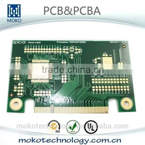
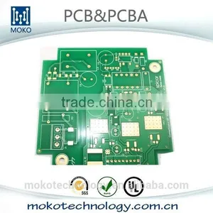
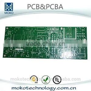
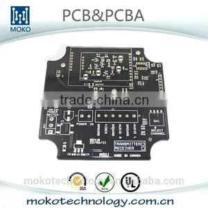
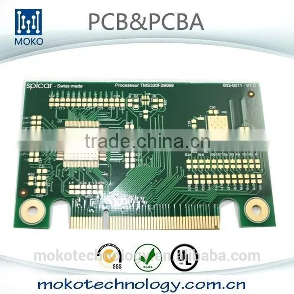
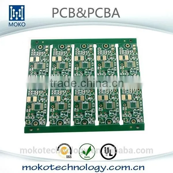
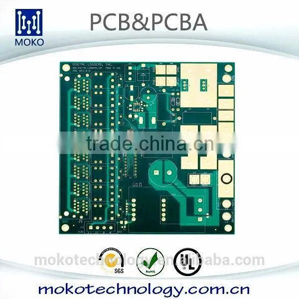
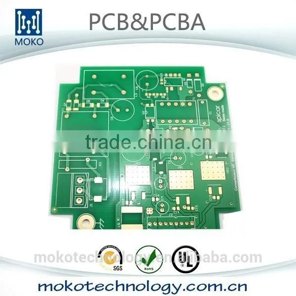
PCB&PCBA Products Show
PCBA from samples to mass production:
PCBA manufacturing steps:
Packing Steps:
PCBAs are packed into plastic bags. Plastic bags are put into small carton. 4 small carton into a big carton.
A big carton with MOKO logo: 35×32×40 cm size.
Shipping Express:

Send Inquiry to This Supplier

You May Also Like
-
China Chaosheng Electronics AI Computing Power Server Multi Layer HDIPCBNegotiableMOQ: 1 Blade
-
PCBA Manufacturing ProcessNegotiableMOQ: 2000 Sets
-
USB Relay Output Module PCB Board for Home AutomationUS$ 1.29 - 2.16MOQ: 1 Piece
-
PCB ,PCBA Service ,one Stop Electronic Manufacturing ServiceUS$ 10 - 100MOQ: 1 Piece
-
Car Wheel Balancing Sensor,wheel Alignment Sensor,wheel Alignment ModuleNegotiableMOQ: 5 Pieces
-
Printed Circuit Budget BoardNegotiableMOQ: 1
-
120M/S ETH Miner Ethereum Dash / DarkCoin X11 Multifunction Ore Chip R9 380 4G Card * 6 Eth Miner Litecoin MinerUS$ 600 - 800MOQ: 1 Piece
-
16D4S 9504 Driver Board for XBOX 360NegotiableMOQ: 10 Pieces
-
PCBA 4GUS$ 100MOQ: 1 Blade
-
3 Hour SMT Stencil Quick Stencil Same Day Stencil Standard, Step, and Nano Coating StencilsUS$ 8 - 300MOQ: 1 Unit


