








 Contact Platform Support
 Help Center
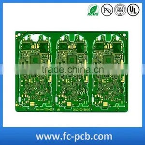
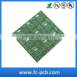
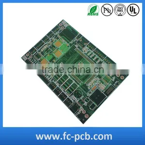
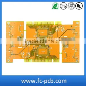
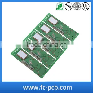
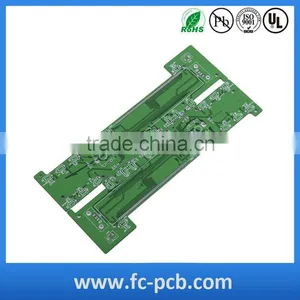
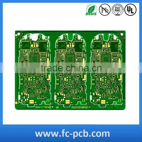
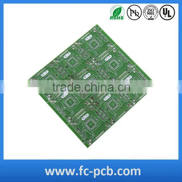
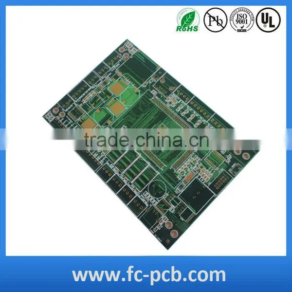
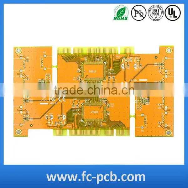
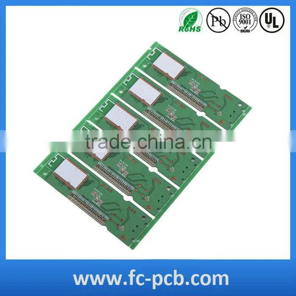
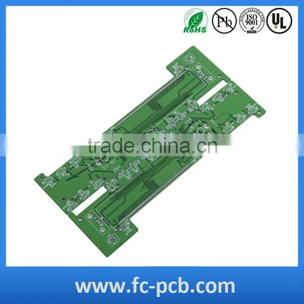
Original Manufacturing Double Sided Pcb Schematic Design


Related Products
-
 Double Side 15*20cm FR4 FR-4 Glass Fiber Blank Copper Clad Printed Circuit Board Universal Prototype PCBUS$ 0.5 - 5MOQ: 1 Piece
 -
Professional PCB Manufacturer/PCB Fabrication From Prototype to Mass ProductionUS$ 1 - 10MOQ: 1 Piece
-
High Precision Printed Circuit Board MakerUS$ 0.1 - 1MOQ: 5 Pieces
-
Rigid Pcb Board,high-density Double-sided Pcb Board,pcb FactoryUS$ 0.5 - 1MOQ: 5 Pieces
-
Double Layer Pcb TV Pcb Board,pcb FactoryUS$ 0.5 - 1MOQ: 5 Pieces
original Manufacturing double sided pcb schematic design
1. Over 12 years' manufacturing experience.
2. UL,ISO9001,ROHS.
3. High-frequency pcb.
4. High quality & fast delivery.
5. OEM one stop service 100% AOI.
Our PCB production capacity
PCB Item |
Manufacture Capacity |
Layer Counts |
1--20L |
Base Material |
FR4,High-TG FR4,CEM3,aluminum,High Frequency(Rogers,Taconic,Aron,PTFE,F4B) |
Material Thickness(mm) |
0.40, 0.60, 0.80, 1.00, 1.20, 1.50, 1.60, 2.0, 2.4, 3.2 |
Max board size(mm) |
1200x400mm |
Board Outline Tolerance |
±0.15mm |
Board Thickness |
0.4mm--3.2mm |
Thickness Tolerance |
±8% |
Minimum line/space |
0.1mm |
Min Annular Ring |
0.1mm |
SMD Pitch |
0.3mm |
Holes |
|
Min Hole Size(mechanical) |
0.2mm |
Min Hole Size(laser hole) |
0.1mm |
Hole Size Tol (+/-) |
PTH:±0.075mm;NPTH: ±0.05mm |
Hole Position Tol |
±0.075mm |
Plating |
|
HASL/LF HAL |
2.5um |
Immersion Gold |
Nickel 3-7um Au:1-5u'' |
Surface Finish |
HAL,lead-free HAL,ENIG,Plated Gold,Immersion Gold,OSP |
Copper |
|
Copper Weight |
0.5--6oz |
Color |
|
Soldermask |
Green, Blue, Black, White, Yellow, Red, Matt Green, Matt Black, Matt Blue |
Silkscreen |
White, Black, Blue,Yellow |
Acceptable File Format |
Gerber file,Powerpcb,CAD,AUTOCAD,ORCAD,P-CAD,CAM-350,CAM2000 |
Certificate |
ROSH,ISO9001,UL |
Our PCBA Competence:
Stencil size/range: |
736x736mm |
Minimum IC pitch: |
0.30mm |
Maximum PCB size: |
1200x 500mm |
Minimum PCB thickness: |
0.35mm |
Minimum chip size: |
0201 (0.2x0.1)/0603 (0.6 x 0.3mm) |
Maximum BGA size: |
74x74mm |
BGA ball pitch: |
1.00mm (minimum), 3.00mm (maximum) |
BGA ball diameter: |
0.40mm (minimum), 1.00mm (maximum) |
QFP lead pitch: |
0.38mm (minimum), 2.54mm (maximum) |
Frequency of stencil cleaning: |
1 time/5 to 10 pieces |
FULLTRONICS CORPORATION LIMITED is a Chinese-owned company based in Shenzhen, established in 2002, We work with our customers in designing and Cloning the electronics for their products. In addition, we manufacture completed PCB,FPC,SMT Assembly,COB Assembly , T/H Through Hole Assembly , Mold and Plastic injection, “box-build” controls that include enclosures, wire harnesses and overlays. Products are functionally tested and sent directly to the end-user.
An example of a typical customer would be one who is developing an electro-mechanical product but does not have the capability to design the electronics portion. We provide support from initial engineering design pecifications through manufacturing the end-product. We also work with customers that have in-house electronic engineering design teams. We assist with design efficiencies, manufacturability, reliability and improving quality during the manufacturing process. In this capacity we act as a contract manufacturer.
Why Fulltronics?
1. Fast quotation time.
2. Stable Lead Time For Production Orders.
3. Flexible Shipping Method and Payment terms:
4. With the greatest care and responsibility to packaging
and send to you 100% functional board products.
5. We are Alibaba Trade Assurance supplier and Gold supplier.
6. Contac us at any time ,we are always on line !
- 1. Are my design files secure when I send them to you?
Your files are held in complete safety and security.Your files are never shared nor will any third parties have access to your design files.Fulltronics can sign an NDA(Non-disclosure agreement) before sending files.
- 2. For small quantity orders, can you produce prototype PCBs?
Yes. Fulltronics can produce prototypes. but the greater the quantity, the greater the cost savings.
- 3. What file formats do you accept for PCB and assembly?
Gerber ,CAM Auto CAD DXF, DWG formats.
- 4. Do you have after-sales product servicing available for your customers?
Yes, for any quality problems Fulltronics will take our responsibility to solve it for you any time.
More details about us, kindly scan website:
If you send us your Gerber Files and PCB specification, we will quote for you within 12 hours.

Send Inquiry to This Supplier

You May Also Like
-
AI Power System PCB+PCBA,backplane Server PCBANegotiableMOQ: 1 Blade
-
PCBA Manufacturing ProcessNegotiableMOQ: 2000 Sets
-
USB Relay Output Module PCB Board for Home AutomationUS$ 1.29 - 2.16MOQ: 1 Piece
-
PCB ,PCBA Service ,one Stop Electronic Manufacturing ServiceUS$ 10 - 100MOQ: 1 Piece
-
Car Wheel Balancing Sensor,wheel Alignment Sensor,wheel Alignment ModuleNegotiableMOQ: 5 Pieces
-
Printed Circuit Budget BoardNegotiableMOQ: 1
-
120M/S ETH Miner Ethereum Dash / DarkCoin X11 Multifunction Ore Chip R9 380 4G Card * 6 Eth Miner Litecoin MinerUS$ 600 - 800MOQ: 1 Piece
-
16D4S 9504 Driver Board for XBOX 360NegotiableMOQ: 10 Pieces
-
Custom PCBA Assembly Service | SMT & Through‑Hole Electronic PCB Assembly Prototype & Mass ManufacturingNegotiableMOQ: 1 Blade
-
SMT PCB Prototype Assembly Service, PCBA Turnkey Manufacturing, Small Batch SMD Soldering, Support 5 Piece Minimum OrderNegotiableMOQ: 5 Pieces


