The design of Printed Circuit Boards (PCBs) is the backbone of modern-day technology and is used in everything from cell phones to industrial machines. If you’re an engineer or a hobbyist, it’s essential to know the basics of PCB design to bring your ideas to life practically. This blog post aims to walk you through the fundamentals of PCB design – its significance, how it is done, the primary processes, and the practices that bolster optimal PCB design in terms of reliability and efficiency. After reading this blog, you will know the right tools and the right approach you need to implement to transform your innovative ideas into reality and build reliable electronic devices.
What is a Printed Circuit Board?

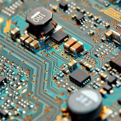
A vital building block of electronic circuits, a Printed Circuit Board (PCB) provides mechanical support and electrical connections for the device’s components. It is composed of a non-conductive board and various elements, such as resistors, microchips, and capacitors. A PCB interconnects electrical components mechanically and electrically as a flat board typically made from non-conductive materials. Thin layers of conductive pathways are etched onto its surface, enabling current to flow among multiple components. PCBs have become indispensable in today’s world due to their size, robustness, and the ability to efficiently assemble an ever-increasing variety of devices, including medical and smartphone equipment.
How do Printed Circuit Boards Function?
Printed Circuit Boards (PCBs) serve as the basis for interfacing electronic devices within different components, providing signals and power for transmission. The board is composed of various layers, including the base material (often fiberglass), a protective solder mask, and a conductive layer, usually made of copper. The conductive traces on the PCB ensure that electricity flows accurately, so signals are relayed to the correct places within the circuit.
A combination of design and assembly always works together to ensure that PCBs are operational. In one, engineers conceptualize and lay out electrical pathways, avoiding significant interference whilst maintaining appropriate impedance levels using specialized software. Components, such as inductors or capacitors, are positioned in the designed spaces, ensuring optimum performance. The components that were placed have to be soldered either manually or automatically to the board to provide secure connections.
For example, modern consumer or industrial-grade PCBs, often used in personal computers or mobile phones, can have up to 30 layers. This innovation helps dramatically improve the efficiency of interconnections, enabling faster signal transmission in data centers or 5G applications. Furthermore, the development of high-frequency laminates, along with other thermal management materials, greatly enhances reliability during harsh conditions.
The global PCB market was worth approximately $60 billion as of 2022, fueled primarily by demand surges from consumer electronics, as well as automotive and industrial electronics. PCBs are crucial in modern electronics, especially with the challenges of powerful and miniaturized devices. Enhancing reliability further augments this, almost at the same rate as systems that need dependability.
What Materials are Used in PCBs?
A Printed Circuit Board (PCB) consists of various base materials that provide it with mechanical strength and dielectric insulation. The core of a PCB is its substrate, which is often FR4. Vinyl foamed sheets combine inexpensive materials like glass fiber and epoxy resin, making FR4 both strong and thermally resistant. Because of its effectiveness, this material is preferred in many areas.
In a PCB, copper is used as a foil for forming layers of conductors. These copper layers are crucial in providing interconnections for the electrical signals across the board. The thickness of the copper foil used is usually between 1 oz/ft² and 6 oz/ft², depending on the requirements. Higher current circuits have greater thicknesses.
Solder mask layers, mostly green, cover the copper layer of a conductive track and serve to insulate and protect the traces from surrounding elements, such as environmental moisture and oxidation. Other protective layers, composed of ink that serves to mark parts and components in a form for easy identification, are called Silkscreens.
Supplementary materials consist of polyimides, which are a flexible and heat-resistant polymer useful in flexible printed circuits (PCBs), and ceramics for high-frequency or elevated-temperature applications due to their thermal conductivity and dielectric properties, for the most advanced PCBs, which incorporate technologies such as 5G and self-driving vehicles, low-loss materials like PTFE (Teflon) are often added to ensure optimal performance at high frequency ranges.
The demand for smaller and more efficient electronics has dramatically impacted the evolution of PCB materials. As of 2023, industry insights reveal that over 70% of multilayer PCBs use high-Tg (glass transition temperature) laminates, indicating the importance of longitudinal electronics and performance efficiency in modern devices, where material selection is crucial and drives advancement.
Why are Copper Layers Important?
Copper layers are essential in printed circuit boards (PCBs) due to their electrical conductivity, thermal properties, and reliability under stress. These layers serve as conduits for electrical signals, and copper’s thermal conductivity helps dissipate heat, which is crucial in preventing damage to components in tightly packed, high-power configurations.
According to industry data, the copper thickness in PCBs ranges from 0.5 to 3 ounces per square foot, depending on the application. For instance, high-current circuits need thicker copper layers, while microfabricated designs for mobile or wearable devices use ultra-thin copper layers. Also, uh, advanced ion plating makes it possible to manufacture multi-layer PCBs with complex copper routing, enabling designs with hundreds of layers for data centers and telecommunication networks. These are examples of copper strips that aid seamlessly in integrating higher-order signals into modern PCBs with more advanced functionality.
How to Approach PCB Design?

Start by defining the specifics of the project, like the size, functionality, and performance requirements, to manage PCB design effectively. Develop a schematic that clearly describes the interrelations of the circuits. Utilizing PCB design software is essential for organizing and placing all parts, as well as optimizing spacing and alignment for manufacturability. Issues with operational execution can be avoided by addressing structural problems, such as signal integrity, power distribution, and heat dissipation. Before moving forward with manufacturing, perform thorough simulations and reviews to verify the design.
What are the Key Steps in PCB Design?
Designing a PCB involves several essential steps to ensure the board works efficiently. The process can be broken down into these steps:
Establishing the Requirements: Start by determining the parameters you need for the design process, such as size, layers, operating frequency, and the type of application for the PCB. Having a clear understanding of these specifications helps provide a roadmap to follow during the design phase and minimizes the chances of incurring expensive changes later on.
Schematic Design: Develop a schematic diagram of the circuits, ensuring that all parts are explained thoroughly and clearly, using up-to-date computer software. This step involves specifying the circuit parts, connections, and the netlist, which outlines how the specific parts of the system interact electrically with each other.
Component Identification and Selection: Choose components based on the parameters specified in the previous step, while also considering their cost, performance, and availability. Check the compliance of the components with the industry standard and ensure they fit within the environmental conditions, design longevity, and power requirements of the board.
Designing the PCB Layout Based on the Schematic: Convert the system’s schematic components into real-world components, translating the schematic’s axial parts into a physical layout. Place components on the PCB optimally, considering signal integrity, and route traces through the shortest paths while meeting impedance requirements and minimizing crosstalk. For high-speed designs, use a board with at least four layers to enhance grounding and signal performance.
Power Distribution and Thermal Management: Incorporate power planes and distribution systems to prevent voltage drops and power losses on the printed circuit board (PCB). Use thermal vias, heat sinks, and a suitable copper thickness to dissipate heat from high-power components effectively.
Design Rule Check (DRC): Perform automated design rule checks to verify that the layout complies with various manufacturing constraints, such as minimum trace width, required distance between traces, and dimensioning vias. Most modern PCB design packages are equipped with sophisticated DRC algorithms that look for more advanced errors.
Signal Integrity and Simulation: Analyze the signal integrity and EMI using simulation tools. Find and fix reflections, crosstalk, ground loops, and many others. Also, for faster circuits, controlled impedance traces and differential pairs should be checked.
Prototyping and Testing: Build the PCB prototype and put it through thorough testing, simulating practical operating conditions. Use oscilloscopes, logic analyzers, and thermal cameras to validate performance and identify problems. Evidence shows that iterative prototyping substantially improves the final failure rates.
Documentation and Manufacturing Preparation: Create all necessary documents for PCB manufacturing, including Gerber files, bill of materials (BOMs), pick-and-place drawings, and assembly drawings. When generated, these files need to be verified against the manufacturer’s instructions to avoid problems during production.
Quality Assurance: Conduct post-manufacturing quality control checks using Automated Optical Inspection (AOI) and X-ray inspection to detect potential manufacturing defects, such as misalignment, soldering errors, or open circuits.
Together with modern technology in PCB design tools and methods, these systematic steps have greatly enhanced the reliability of PCBs and shortened the design cycles. Attention to detail at every level reduces risks and ensures the final product operates precisely within its intended specifications.
How does Signal Integrity Affect Performance?
Backup, maintaining optimal signal integrity, reinstates itself as one of the biggest challenges that must be overcome when prioritizing the utmost accuracy and performance for contemporary electronic systems. Device escalation in terms of speed and frequency only adds fuel to the fire, as poor signal integrity is associated with data errors, system malfunctions, and performance degradation. Numerous parameters, defined in time and space, such as signal timing, noise, crosstalk, and even electromagnetic interference (EMI), can affect the quality of signals sent and received on printed circuit boards (PCBs).
For example, new research claims that poor trace layout design is a reason for signal degradation, which results in timing mismatches and skew. This causes issues with data integrity in high-speed interfaces, such as PCIe lanes and memory buses, that are lower than or equal to DDR5. Advanced protocols like 5G mark an evolution in mobile telecommunication interfaces, where more significant attention to detail becomes pivotal. The lack of precision destroys the clarity of real-time communication and gives rise to latency complications that undermine the efficacy of these communications. Reports suggest that at operating frequencies over 1 GHz, minor flaws in PCB materials become highly problematic. Variations in dielectric constants showcase the gap in material selection, as reflection and loss of transmission become rampant.
Impedance matching is needed to preserve the integrity of signals. In any signal pathway, inconsistent impedance can create signal reflections and power loss, particularly at high frequencies. Some methods, such as simulations and proper terminations, solve these problems by maintaining a consistent impedance along the path.
Engineers do an astounding amount of work to ensure that signals and their elements function without interference due to time and signal distortion. Now, thanks to the advances in testing and simulations, such as TDR and software modules for signal simulation, designers can more efficiently guarantee the preemptive resolution of any potential signal integrity problem.
What Tools are Available for PCB Design?
The design process in PCB layout has seen numerous advancements, supported by various tools to improve efficiency. Some of the widely adopted ones are given below:
Altium Designer: Altium Designer integrates schematic capture alongside PCB layout, FPGA design, and even embedded system software into one cohesive stripped PC, allowing for complete mobility within the system. Seamless work is enabled without needing to switch between tools, which significantly reduces the likelihood of errors while increasing workflow efficiency. Professional and complex projects are accomplished with ease thanks to Altium Designer’s advanced features, including complex routing, 3D visualization, and advanced collaborative tools.
Eagle (by Autodesk): The user-friendly interface allows novice users to easily familiarize themselves with fundamental concepts, as well as for hobby projects and small businesses. Eagle features components, editing schematics, laying out the PCB, and an auto-router. Ample community support combined with an extensive library of components makes it a perfect entry point.
KiCad: KiCad is a free, open-source PCB design tool that is popular for its rich feature set. It supports multi-layer PCB design, 3D viewing, advanced library management, and more. Continuous updates from contributors increase the tool’s value for both small and professional projects.
Mentor Graphics Xpedition (Siemens): Mentor Graphics Xpedition specializes in high-end capabilities for peripheral Add-Ons, advanced PCBs, and Advanced Multi-board systems. It comes with powerful Advanced Signal Integrity, Thermal, and Power Integrity tools. For advanced multi-board or complex systems, Xpedition is often adopted because of its integration and collaboration features.
OrCAD (by Cadence): One of OrCAD’s prominent advantages is its powerful simulation features for analog and mixed-signal circuits, which aim to ensure seamless interoperability. In particular, it has remained a leader in the PCB market for a long time due to its expertise in circuit simulation. In addition to the PCB layout, it enabled engineers to optimize designs, allowing them to test the circuits during the build phase.
Fusion 360 Electronic Design: Mechanical CAD and PCB design have now been integrated and centralized to one platform, collectively referred to as Fusion 360. This allows for smoother electronics and mechanical workflows, which are necessary for products with mechanical bodies that contain complex electronic components.
Proteus Design Suite: Proteus PCBs with embedded microcontrollers are best for designing and simulations. Its simulation capabilities are best for exploring and confirming circuit behaviors before physical prototyping.
Many of these tools offer advanced features, such as improved collaboration for remote teams and AI-assisted layout recommendations, which can simplify work processes. The scope, intricacy, and particular needs of the project at hand usually determine a designer’s selection of tools. Therefore, designers require assessing tools tailored to their exact specifications.
What are the Types of Printed Circuit Boards?

Different types of PCBs, or Printed Circuit Boards, serve various functions. The main types include:
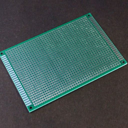
Single-Sided PCBs: Electronically, the most basic. Thoroughly used for simplistic devices, these boards have only one side of conductive material. Often provide the best value for money, as they are low-cost.
Double-Sided PCBs: These are the next step in complexity, featuring conductive materials on both sides. Can allow for vias and thus provide connections between components on both sides. More complex circuits can be made with these.
Multi-Layer PCBs: Superior to double-sided boards, multilayer pieces provide even more layers of conductive materials with which components can interface. Designed for advanced electronics, these allow for greater circuit density and enhanced functionality.
Rigid PCBs: Sturdier boards that still allow for some flexibility of construction. It can be used in devices that require a fixed orientation of components.
Flexible PCBs: Used in devices that are smaller or require complex component arrangements. Allow for bending to various shapes, aiding in portability.
Rigid-Flex PCBs: Gaining popularity due to their flexibility and sturdiness in a configuration in which they are fixed and often used in things like space equipment or medical machinery for reliability.
Every type of board is selected with the complexity of its design, its functions, and the required performance in mind, and seeks to accomplish all these goals to the best of its ability.
What is a Rigid Printed Circuit?
A Rigid Printed Circuit Board (Rigid PCB) refers to a type of printed circuit board made of a solid dielectric substrate, which provides structural support and ensures the board maintains its shape under various conditions. Unlike flexible PCBs, rigid PCBs do not bend and are used in more permanent electronic devices, such as computers, mobile phones, and televisions.
Rigid PCBs are made up of several layers, including a substrate, which is most often made of fiberglass, a copper layer that conducts electricity, a solder mask to protect the conductive circuits, and a silkscreen for labeling components. They are famous for being highly durable, high-performing, and able to sustain complex circuit designs.
New information indicates that the sales of rigid PCBs continue to rise, with steady interest coming from the consumer electronics, automotive, and telecommunication sectors. More advanced methods of manufacturing achieve compact and reliable designs, making rigid PCBs crucial components in devices that require precision and durability, such as in automotive control systems that rely on rigid PCBs for their reliability. In addition, the ability of the rigid PCBs to support multi-layered designs boosts their multi-functional capabilities, making them more desirable in modern electronics.
How do Flexible Substrates and Rigid PCBs Differ?
There are notable differences between flexible substrates and rigid printed circuit boards (PCBs) in terms of structure, application, and performance characteristics. Flexible substrates are made from materials such as polyimide or polyester, which are easily bendable. These materials are helpful in applications that involve dynamic movement, such as wearable devices, smartphones, and aerospace components. Unlike rigid PCBs, flexible substrates can conform to 3D spaces, which helps minimize the size and weight of electronic devices.
Rigid PCBs use solid, non-flexible materials such as fiberglass, which gives the board mechanical stability and durability. They are most often used in devices that require high structural integrity, such as computers, automotive systems, and industrial machines. Rigid PCBs make it possible to have multi-layered designs, enabling complex and dense circuitry essential in advanced computational electronic devices.
Furthermore, it has been shown that flexible substrates are often more reliable in applications with mechanical stress, because they can bend and vibrate without failure. However, they are weaker in heat resistance and more expensive to manufacture than rigid PCBs, which limits their use in high-power and thermally demanding applications. Rigid PCBs are cheaper and withstand heat better, but are inflexible in compact or non-standard configurations, which makes them less desirable. Both technologies serve critical functions in contemporary electronics and are often used together within the same system to optimize performance in various applications.
What is a Metal Core Printed Circuit?
It’s also referred to as a thermal printed circuit board (PCB). A Metal Core Printed Circuit Board (MCPCB) is one type of printed circuit board (PCB) that has a metal layer, usually copper, aluminum, or an alloy of metals, incorporated in the middle. This core metal layer is designed to effectively remove heat from an electronic component, making MCPCBs valuable for high-power and thermally sensitive applications.
The thermal conductivity of MCPCBs is key to their advantages, as they have high thermal conductivity ranging from 1.0 W/mK to 12.0 W/mK, or even higher, depending on the particular material. It also enhances dependability and increases the system’s lifespan. This means that critical components such as LEDs, power transistors, or high-speed integrated circuits (ICs) can be placed on the MCPCB. For example, aluminum-core boards are commonly used in LED lighting systems as they achieve maximum luminous efficacy and reliability at preferred ambient temperatures.
MCPCBs incorporate a dielectric layer that provides electrical insulation and enables the thermally conductive transfer of heat to the metal core. In the case of industrial power equipment and solar energy systems, PCBs with copper cores are preferred since they provide superior thermal conductivity and current-carrying capacity. Aluminum-core boards are more cost-effective and widely used in consumer electronics, automotive lighting, and communication devices due to their balanced performance.
Compared to other active or passive cooling techniques, MCPCBs offer greater compactness and higher component density, a desirable trait for modern electronics. Continual progress in materials science and manufacturing will further refine MCPCBs, helping to build more advanced electric smart devices, electric vehicles (EVs), and renewable energy systems that require reliable thermal management solutions.
How is a PCB Manufactured?
The creation of a Printed Circuit Board (PCB) requires multiple steps to guarantee its accuracy and functionality:
Designing the Layout: Using particular design software, an engineer designs and arranges the components and circuitry on the PCB.
Preparing the Substrate: The base material, generally composed of fiberglass, has a thin film of conductive copper applied to it.
Patterning the Circuit: A photoresist layer is deposited. After that, the UV light transfers the design onto the board. After the negative tape is stuck on, the unwanted copper portions are removed in the etching bath.
Drilling and Plating: The copper-plated holes are drilled for component leads or vias, and copper plating is applied to these holes to establish electrical connections between the different layers.
Solder Mask Application: A solder mask is applied. This prevents the paths that will be connected from the conductor tracks from causing short circuits when soldering.
Component Assembly: Operators manually or automatically place the components onto the PCB and solder them into position for efficient electrical connections.
Inspection and Testing: The assembled PCB is then tested to check its functionality against standards.
The above procedure combines accuracy and precision, ensuring PCBs that are fit for various functions.
What are the Steps in Printed Circuit Board Manufacturing?
The steps in manufacturing a PCB have some crucial stages. First, I concentrate on laying out the design and making the corresponding design files. Later, I chose the board material and laminated the layers of the PCB together to form a solid block. At this stage, I also create holes for mounting and via placement, which are later on patterned through plating and etching. After that, the solder mask is applied and the circuitry is protected until components are mounted and soldered. Finally, the board undergoes inspection and testing to ensure that all criteria have been met and are operational.
How do Thermal Expansion and Conductive Material Affect Manufacturing?
The thermal expansion and the characteristics of the materials used in producing PCBs are of great importance. During the operation or soldering of a printed circuit board, it undergoes one or more cycles of temperature changes, which cause different materials to expand and contract. Parts of a PCB, such as copper, fiberglass, and epoxy, are made from various materials and have different coefficients of thermal expansion (CTE). If these differences are too significant, the CTE mismatch can stress the PCB, potentially warping it, cracking solder joints, or leading to failures in plated-through holes (PTH).
For example, one of the most essential Conductive parts of a circuit board is copper, and its CTE is around 16.5 ppm/°C. The range of CTE values for FR-4 composite used as base material is about 10 to 20 ppm/°C in the X-Y plane, but in the Z-axis it can rise to around 70 ppm/°C. This isn’t easy when dealing with high-temperature steps, such as reflow soldering, which can go above 200°C.
Innovations in materials and techniques are being developed to target these problems directly. To maintain temperature stability, polyimides and fiberglass with a low coefficient of thermal expansion (CTE) are useful in composites. Thermal vias and heat sinks are also commonly used to remove heat effectively. Also, controlled CTE designs help decrease the mechanical strain in multilayer structures, which dramatically improves reliability.
Concern about thermal expansion is critical in fields such as aerospace, automotive, and telecommunications, where PCBs undergo significant temperature changes. Applying a specific and correct material selection, along with design methods, allows the manufacturer to produce a reliable product in terms of performance and longevity.
What is the Role of Vias and Traces?
The PCB design also includes vias and traces, which are crucial. Traces serve as conductive pathways made out of copper, which enable the flow of electrical signals between components on the PCB. They also ensure signals are not lost during their travels. The spacing and width of each trace must be appropriate so that current flow is managed without overheating or interference.
At the same time, Vias act as vertical connectors between different layers of the PCB. They allow for the passage of electrical signals and power through the various layers of the board, making it possible to have multifaceted circuit designs in tight areas. There are different types of vias, such as through-hole vias, blind vias, and buried vias. Blind vias enable the connection of outer layers to internal layers, while buried vias only connect internal layers, thus allowing for flexible designs while preventing external complexity from increasing. Applications that fall under the high-frequency category require via and trace layouts to be as precise as possible to avoid signal degradation or loss. Evidence indicates that inefficient vias or trace designs may create an impedance mismatch, resulting in signal reflections and degraded performance. With the addition of techniques like controlled impedance and proper via tailoring, a manufacturer’s PCB capabilities can be further enhanced. Also, the incorporation of microvias in HDI boards aids signal routing while minimizing both size and the number of layers, which is essential in modern electronics like cellphones and devices for high-speed communication.
How to Ensure PCB Reliability?
To achieve PCB reliability, the following practices should be given special attention:
Selection of high-quality materials: Ensuring high-grade substrates, copper, and solder masks helps mitigate material failure risks.
Design for manufacturability (DFM): The PCB must be designed within the bounds of manufacturability to reduce possible defects.
Thermal management: Proper spacing and the use of heat sinks must be implemented to mitigate overheating risks during service.
Testing and inspection: The board must undergo complete tests, primarily electrical, mechanical, and environmental stress testing, to ensure it functions properly.
Proper assembly techniques: Soldering must be performed with precision, and only reliable components must be used to prevent connectivity issues.
Sustained implementation of these practices will significantly boost the reliability as well as the life span of a PCB.
What are the Best Practices for PCB Assembly?
Strategic placement of components is critical for both performance and manufacturability factors. Components with high frequencies, for example, need to be spaced closely together to avoid signal loss due to delays. Furthermore, sensitive components must be placed away from noisy sections to limit interference. A lack of proper spacing and alignment may increase failure rates by 30%.
Thermal Management Techniques: Preventing damage to various parts on the PCB and extending its lifespan requires managing the heat generated from its operation. Use of thermal vias, heat sinks, or copper planes makes heat distribution more reliable by enhancing its flow. Thermal vias have been proven to improve heat dissipation efficiency by 20%.
Optimized Soldering and Reflow Processes: Strong joints, which are mechanically stressed, need the reflow process to maintain specific temperatures for the precise application of solder paste. The AOI and X-ray systems can automate inspections and perform checks on board soldering, saving time and reducing the production error rate.
Ensure Proper Layer Stack-Up Design: Signal performance, along with EMI, is greatly enhanced through the construction of the layer stack-up. Power and ground planes, if used interchangeably, act as natural shields to improve crosstalk amongst high-speed designs. Construction analysis performed on stack-up configurations during the design phase of production helps reduce the number of iterations.
Implement Design for Manufacturing (DFM) Checks: Performing DFM checks guarantees that the PCB design is within the boundaries of manufacturing capabilities. This entails checking the fabrication specification limits, such as trace width, drill sizes, and pad spacings. Following these practices not only ensures manufacturability but also reduces cost and time.
By combining these advanced practices with the latest industry standards, manufacturers can optimize assembly steps, reduce defect rates, and produce high-quality, reliable printed circuit boards (PCBs) for advanced technologies.
How to Test Printed Circuit Boards for Reliability?
Assessing the reliability of printed circuit boards (PCBs) involves applying several standardized techniques to evaluate their functionality in various simulated real-world scenarios. These techniques ensure that the board can sustain operational stresses over time while providing service. Some of the most advanced and effective testing techniques include:
Thermal Cycling Tests: Thermal cycling tests how well the board endures extreme temperature changes. These methods help identify potential solder joint or trace failures over time and repetitive changes in temperature between -40 and 125 Celsius.
Vibration Testing: Solder joints on PCBs for automobiles, aerospace units, and heavy industrial machinery routinely encounter repeated vibrational stresses and shocks, which makes this type of machinery prone to vibrations.
Data shows that boards meeting the standards set by IPC 9701 demonstrate sustained applicability during extended use, despite mechanical shocks.
Insulation Resistance Testing (IR): Evaluating insulation resistance measures helps gauge the dielectric characteristics of the PCB materials. High insulation resistance (in megohms, MΩ) indicates a low risk of electrical leakage. Industry specialists, for instance, suggest that in specific harsh environments, maintaining insulation resistance above 100 MΩ is recommended to avoid a significant drop-off in functionality.
Solderability Testing: The reliability of connections is a critical aspect in PCBs. Wetting balance testing is the most favorable in assessing solderability. It measures the bonding between solder pads and components to ensure proper adhesion. Failure to correct for poor solderability can lead to open-circuit failure, which affects more than 60% of the PCB and is quite operationally sound.
Environmental Stress Screening (ESS): ESS is a newly developed procedure composed of thermal cycling, humidity, and power cycling to assess latent defects. An 85% humidity test at 85°C simulates the long-term impact of aging. Such screening has proven to be effective in reducing field failure rates by 20%.
Automated Optical Inspection (AOI) and X-ray Testing: Manufacturers who use AOI systems have described them as fast and precise for detecting misaligned components and insufficient soldering. This is combined with X-ray testing, which reveals hidden defects such as voids in solder balls or internal layer misalignment.
Implementing careful PCB testing ensures manufacturers’ PCs are reliable and compatible with different working environments. As technology continues to develop, testing standards such as IPC-A-610 and IPC-6012 enable engineers to incorporate better reliability and added features into their designs.
What are Common PCB Design Mistakes?
Developing a printed circuit board (PCB) entails a lot of detailed attention because even the simplest mistakes can create expensive ramifications or create systematic issues during production and operation. Listed below are some common blunders made when designing a PCB, along with their effects.
Faulty Placement of Components: Components placed too close to each other, without regard for thermal management or positioning, could lead to overheating and signal interference. For instance, high-power components should be spaced adequately to prevent overheating or paired with effective heatsinks to improve heat dissipation. Insufficiently planned thermal management can reduce a PCB’s lifespan by a fifth, according to studies.
Tight Spacing and Narrow Trace Width: Too small spacing between traces, as well as narrow spacing, can result in overheating or short-circuiting. Following IPC-2221 guidelines, the trace width must be proportional to the current it carries and the thickness of the copper used. Ignoring this provision could lead to poor conductivity and worsened performance.
Overlooking Ground Return Paths: Failing to incorporate return pathways, especially for high-speed signals, can create electromagnetic interference (EMI) problems. Deficient ground planes and poor layout design lead to a reduction in reliability, as they increase noise and worsen signal integrity, resulting in reduced compliance with EMI testing.
Signal Overloading in a Single Layer: Having too many signals on a single layer of a PCB can lead to troublesome routing problems. It raises the likelihood of crosstalk interference, as well as other issues that stem from the overlapping of traces. The layer stackup must be very carefully balanced to reduce these problems. For instance, routing high-speed signals over several layers with a dedicated ground plane will aid significantly in preserving their integrity.
Ignoring Design for Manufacturability (DFM) Guidelines: Designing with DFM rules ensures the design is fabrication-friendly. Common infringements include placing vias too close to pads, which can cause solder bridging, or using the wrong compliant hole sizes. From DFM analysis for production data, violations had risen. DFM rules estimate an increase of up to 30 percent of production cost just in rework or adjustments to the Defect Services Process.
Failure to Assign Clear Test Points: Failing to set defined boundaries for individual areas of a circuit board means losing the ability to conduct efficient functional testing. Strategic test point placement makes manual diagnostics easier. Throughout the production process, test points facilitate checks for each step, within the manufacturing or quality control phase.
Ignoring Signal Integrity: Without adequate control of impedance, high-speed designs may experience signal skew, signal mismatch, and signal reflections. For example, circuits with long traces and no impedance matching tend to have delays that can break the circuit.
Use of Wrong or Outdated Library Parts: Footprint and connectivity errors may occur when using unchecked library components. Designers are required to perform regular updates on component libraries and audit footprint files against datasheets to mitigate costly mistakes.
Avoiding the cited mistakes allows designers to improve the reliability and performance of their PCBs, decrease costs, and prevent schedule delays. Following a standardized cross-checking process, including DRCs and simulations, enhances precision and standards control.
What are High-Density Interconnect (HDI) PCBs?
High-Density Interconnect (HDI) PCBs are precision-engineered to house a large number of components in a limited area. They have finer traces, smaller vias, and compact pads, which increase the overall functionality of space-constrained designs. Moreover, HDI PCBs are extensively used in smartphones, tablets, medical devices, and similar other devices where high-performance components need to be miniaturized. These PCBs provide improved signal integrity, faster transmission speeds, and the capability to integrate modern chipsets.
What Makes High-Density Interconnect Unique?
High-Density Interconnect (HDI) PCBs are the absolute best due to their advanced features and techniques that outperform traditional PCBs. An example of these features is the microvias, which have a diameter of less than 150 microns. As a result, a more significant number of connections can be made in small spaces. This also helps to improve routing density and increases the number of components that can be placed on a smaller board.
Another defining feature of HDI PCBs is that they accommodate finer line widths and spacing, typically 50 microns or below. This particular precision enhances electrical performance, minimizes signal loss, and ensures reliable operations even at high frequencies. Moreover, HDI technology includes stacked and staggered via connections that help manage complex circuitry.
The telecommunications, automotive, and consumer electronics industries are the leading consumers of HDI PCBs, driving demand for them. For example, the global HDI PCB market was approximately $11.2 billion in 2022, with projections estimating a compound annual growth rate of more than 10% through 2030. The skyrocketing demand can be explained by the requirements for advanced 5G technologies, IoT devices, and other modern computing systems.
What makes HDI PCBs stand out is their ability to overcome industry challenges, such as reducing size and weight while optimizing performance, all without compromising durability or reliability. With these innovative advancements, HDI enhances performance for more complex uses across various industries.
How do HDI PCBs Enhance Component Placement?
By integrating advanced micro via geometries, such as microvias, blind vias, and buried vias, HDI PCBs enable increased wiring density, which enhances component placement. Their ability to incorporate various design features makes them particularly useful for modern electronics that have space constraints. A good example is the use of microvias, which significantly increases the available surface area by lessening the interconnection space needed.
Moreover, the use of advanced materials along with thin dielectric layers in HDI PCBs helps reduce the spacing between components. This not only enhances the reliability of the connections but also enables the transmission of high-frequency signals without any interruptions. Industry studies have shown that HDI PCBs can reduce board size by 50% while increasing component density by 200%, which is beneficial in smartphones, wearables, and aerospace systems. Such innovations help strike a balance between weight and power, keeping up with the high-performance standards needed in today’s technologies.
What are the Advantages of Using HDI Technology?
HDI technologies well support the modern use of electronics since they provide numerous advantages. Ease of miniaturization ensures the career growth of modern electronics, such as lightweight and portable devices. Due to the efficient use of space on the board, HDI PCBs enable advanced implementations in smartphones, tablets, and novel IoT devices. Finer lines and spaces, smaller vias, and greater pad density accomplish this.
While several other technologies allow for proper miniaturization, HDI technology stands out the most because it aligns with faster signal transmission. Efficiency in transmitting signals, along with enhanced integrity, works in favor of a device, especially in complex multilayer devices. It’s safe to say that with HDI PCBs, functionality takes precedence. With 20% additional I/O connections per square inch than standard PCBs, overall performance and potency of electronics are insurmountable.
Intense mechanical stress, along with extreme external conditions, calls for cutting-edge technologies. The lightweight and high durability of HDI PCBs allow for systems that perform well under severe conditions. This is particularly life-changing for the aerospace and automotive industries, where relying on stable temperature control is critical. The enhanced material, combined with an optimized component arrangement, facilitates better thermal management, allowing for more ideal temperature control. Lastly, HDI technology enables long-term cost efficiency. Although the manufacturing cost is high initially, the reduced need for additional layers and enhanced energy efficiency, coupled with improved reliability, results in lower maintenance costs for the product throughout its lifecycle. As the demand for smart devices and other high-performance electronics grows, HDI technology continues to be a critical innovation that propels growth in the industry.
Reference Sources
The following is research related to printed circuit boards (PCBs), highlighting the latest advances and approaches:
-
“Printed Circuit Board Structural Properties and Spiral Groove Trace Conductors for Hydrodynamic Gap Maintenance in Axial Flux Rotating Machines” (2019)2:
- Key Findings: This study examines the use of PCBs in axial flux rotating machines, focusing on their structural properties and the integration of spiral groove trace conductors to maintain hydrodynamic gaps.
- Methodology: The research combines electric and electromagnetic field theory with thermal properties to address mechanical challenges in PCB-based machines.
-
“Printed Circuit Board (PCB): Design and Test” (2019)3:
- Key Findings: This paper discusses the application of deep learning for optical detection of hidden hardware Trojans during PCB manufacturing, enhancing cybersecurity in electronics.
- Methodology: A deep learning framework was developed to identify and benchmark hardware Trojans, with a focus on optical inspection techniques.
-
“Designing and Planning a Printed-Circuit Board (PCB) Prototype” (2006):
- Key Findings: Although older, this study provides a comprehensive guide on planning PCB prototypes, addressing design complexities and testing strategies.
- Methodology: The authors emphasize early-stage planning, including equipment selection and strategically placing test points.
Frequently Asked Questions (FAQs)
Q: What is a Printed Circuit Board (PCB), and where are printed circuit boards used?
A: A Printed Circuit Board (PCB) is a board used to mechanically support and electrically connect electronic components using conductive traces, pads, and other features etched from layers of copper sheets laminated onto a non-conductive substrate. Printed circuit boards are used in a wide variety of applications, including consumer electronics, automotive systems, and medical equipment.
Q: What is the role of dielectric material in PCB design?
A: Dielectric material in PCB design serves as an insulating material that allows electrical signals to pass between layers without interference. It provides the necessary insulation between conductive layers and helps maintain signal integrity.
Q: What are high-density interconnect (HDI) PCBs?
A: High-density interconnect (HDI) PCBs are printed circuit boards that have a higher wiring density per unit area compared to traditional printed circuit boards (PCBs). They make use of finer lines and spaces, smaller vias and capture pads, and higher connection pad density to accommodate more PCB components in a smaller area.
Q: How do rigid and flexible PCBs differ?
A: Rigid PCBs are made from solid substrate materials that do not bend, providing structural support to the board designs. Flexible PCBs, on the other hand, use materials like woven fiberglass cloth that can bend and flex, allowing them to fit into compact or irregular spaces.
Q: What materials are commonly used as substrate materials in PCBs?
A: Common substrate materials in PCBs include FR4, a composite of woven fiberglass cloth with an epoxy resin binder, and metal-core substrates that enhance thermal management. These materials provide the structural and electrical foundation for the board.
Q: What are the differences between surface-mount and through-hole components?
A: Surface-mount components are mounted directly onto the board’s surface, allowing for more compact board designs and higher component density. Through-hole components have leads that pass through holes in the board, providing strong mechanical connections and are often used for passive components.
Q: What is the significance of using layers of copper in PCB design?
A: Layers of copper in PCB design are crucial for forming the conductive traces and pads that make up the electrical connections on the board. Multiple layers of copper allow for more complex circuitry and greater design flexibility.
Q: How does the printed circuit board fabrication process begin?
A: The printed circuit board fabrication process begins with creating a design layout, which is then used to produce a photomask. This mask is used to transfer the circuit pattern onto a copper-clad board, which is later etched to create the conductive traces.
Q: At what point is the board considered ready for testing and assembly?
A: The board is ready for testing and assembly once all the layers and components have been correctly aligned, applied, and soldered in place. This includes verifying that all electrical connections are intact and the board meets the required specifications.
Q: Can PCBs be 3D printed?
A: Yes, PCBs can be 3D printed using specialized techniques and materials that allow for the creation of conductive and insulating layers. However, this method is generally less common and typically used for prototyping or low-volume production.